
PCB design software
PCB design is an important part of the product development process, and it continues to evolve and change as electronics become more prevalent and more complex. On this page you can learn the ins and outs of PCB design software directly from the experts at Siemens.
What is PCB design software?
PCB design software refers to computer applications specifically designed to facilitate the creation, layout, routing, simulation, and analysis of printed circuit boards (PCBs). These software tools provide a platform for engineers to complete PCB designs. What is PCB design? Learn more in our blog!

Why is PCB design software important?
Device functionality
PCB design software helps ensure that these components like microprocessors, memory & sensors work together and that the device will work as intended.
Product size
PCB design plays a role in determining the size and form factor of electronic devices. Compact and efficient PCB layouts done in PCB design software allow for smaller and more portable devices.
Signal Integrity
PCBs are responsible for routing signals between components. The right PCB design software can help you design boards that minimize signal interference, ensuring data and power transmission is reliable and stable.
What can PCB design software do for you?
PCB design software should deliver the functionality you need, like layout and schematic, but also go beyond to enable a fully integrated electronic systems design flow that bridges the gap from design to manufacturing with integrated verification at every step.
PCB design software from Siemens


Digitally integrated & optimized
Establishing a digitally integrated solution across multiple engineering domains reduces manual intervention, fosters collaboration and improves transparency across disciplines. Learn more about how to create a digitally integrated and optimized multi-domain environment.
Engineering productivity
Using today’s PCB design tools like Xpedition can significantly optimize the design approach and facilitate multi-discipline integration and collaboration so that you can be faster, produce higher quality designs, and even lower project risks.
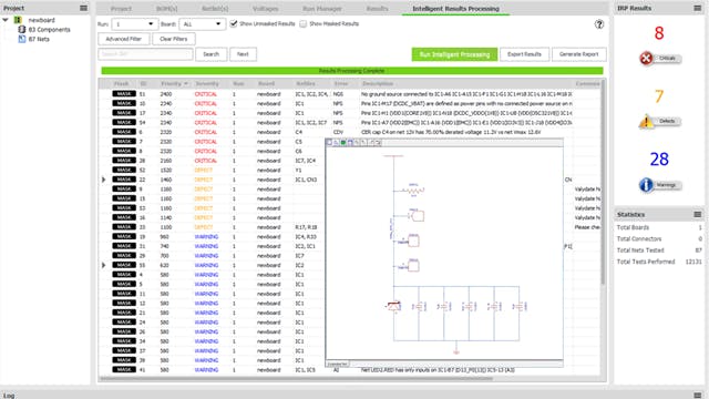
Digital verification
Shift-left design methodology integrates design verification tools throughout the PCB design process to let designers find and fix errors where they happen, instead of waiting until later.
.png?auto=format,compress)
Model-based systems engineering
A digital thread breaks down barriers between teams and establishes traceability from requirements all the way through manufacturing and across multiple design domains. A digital twin allows teams to perform simulations early, enabling trade-off analysis and optimized system integration.

Supply chain resilience
Electronic systems design companies have always depended on a value chain of suppliers and manufacturing services to bring successful products to market. Connecting the demand for a product with the supply of its necessary parts has never been more complex than it is today.
Abaco Systems | AMETEK
Facilitating product innovation through tools, processes, and people
Company:Abaco Systems | AMETEK
Industry:Electronics
Location:Huntsville, Alabama, United States
Siemens Software:HyperLynx, Valor NPI, Xpedition Enterprise
The tools themselves are a very important aspect of what we do here. It may be that a lesser tool could be employed but the time scales involved in that would just be horrific. We need the fastest most efficient tools that we can have to get our very complex designs to market on time. We get that from the Siemens tools.
Frequently asked questions
What are the key features of PCB design software?
PCB design software should offer an intuitive and user-friendly interface along with robust design tools for schematic capture, layout, routing, design for manufacturing (DFM) analysis, and simulation. It should seamlessly integrate with other design tools and formats to facilitate collaboration and streamline the design and engineering process. Built-in features such as design rule checking (DRC), DFM analysis, signal integrity (SI) & electromagnetic compatibility (EMC) analysis, power integrity (PI) analysis, and thermal analysis help identify and rectify potential issues early in the design process, ensuring manufacturability/producibility, reliability, and optimal performance. Efficient library and data management, version control, collaboration tools, manufacturing outputs and documentation capabilities further enhance productivity and accuracy, while access to comprehensive customer support and an active user community provides assistance and fosters knowledge sharing among users.
How does PCB design software help in optimizing printed circuit board performance?
PCB design software optimizes PCB performance through a range of features and tools. The software provides intuitive interfaces and robust design tools for schematic capture, layout, routing, DFM analysis, and simulation, enabling designers to create PCB layouts that meet performance requirements. Built-in capabilities such as DRC, SI and EMC analysis, PI analysis, and thermal analysis help identify and address potential issues early in the design process, ensuring optimal signal integrity, EMC, power distribution, thermal management, and manufacturability. Additionally, integration with other design tools and formats streamlines the design process, while features like library/data management, version control, collaboration tools, manufacturing outputs, and documentation capabilities enhance productivity and accuracy. Overall, PCB design software empowers designers to create complex high-performance PCBs that are reliable, manufacturable with high yields at the lowest cost, and meet design specifications.
What are the different types of PCB design software available in the market?
- Commercial PCB design software: These are professional-grade PCB design tools offered by software companies for a wide range of applications. Examples include Siemens Xpedition and PADS Professional.
- Free/open-source PCB design software: These are PCB design tools available for free or with open-source licenses, often with robust features and active user communities, but are limited in their capabilities and features when compared to commercial PCB design software.
- Cloud-based PCB design platforms: These platforms offer PCB design capabilities accessible via web browsers, allowing collaboration and design work from anywhere with an internet connection. Xpedition and PADS Professional can both be cloud-connected.
What factors should be considered while choosing PCB design software?
Several factors should be carefully considered when choosing PCB design software. Firstly, the software's capabilities and features, including schematic capture, layout, routing, simulation, and analysis tools, should align with the project requirements and design objectives. Compatibility with other design tools, file formats, and manufacturing processes is essential for seamless integration and collaboration. Additionally, ease of use, user interface intuitiveness, and learning curve play significant roles in productivity and efficiency. It’s also important to also consider a tool that will not be outgrown due to the increasing complexity of future projects along with the evolution of internal ecosystems, and continued industry evolution. Consideration should also be given to the software's support, documentation, and availability of resources such as tutorials and forums.
Can PCB design software handle complex designs and high-speed signals?
Yes, modern PCB design software is equipped to handle complex designs, high power designs, and high-speed signals effectively. These software packages offer advanced features such as tightly controlled signal routing and tuning, impedance control, wave guide via stitching, signal integrity analysis, and high-speed design rule checking (DRC) capabilities to ensure optimal performance of high-speed signals. Additionally, they provide tools for simulation and analysis, allowing designers to identify and address potential signal integrity issues early in the design process. Advanced tools have the capability to create and reuse design templates and DRC templates to save time from having to re-invent the wheel.
Some advanced software tools have the capability to incorporate a team design approach by allowing multiple users to work on one main design concurrently (at the same time). This approach significantly reduces engineering design cycle time while maximizing team utilization.
PCB design software can support complex multi-layer boards, high-density interconnects, multi-via structures, and intricate layout requirements, enabling designers to tackle even the most complex PCB designs with confidence and precision.
What PCB design software does Siemens offer?
Siemens offers the following PCB design software:
- Xpedition: Xpedition is a high-end PCB design software designed for enterprise-level ecosystems and for design teams tackling tomorrow’s complex PCB projects today. It provides advanced capabilities of multidomain and multidiscipline system level integration for schematic design, layout, routing, simulation, and analysis, along with integrated collaboration and data management features, to include supply chain intelligence at the point of design.
- HyperLynx: HyperLynx is a simulation and analysis toolset for signal integrity, power integrity, and electromagnetic interference/compatibility (EMI/EMC) analysis. It helps designers optimize high-speed designs, validate signal integrity, power integrity, and ensure reliable performance and is integrated with both Xpedition and PADS Professional.
- PADS Professional: PADS Professional is a comprehensive, optionally cloud-connected PCB design solution suitable for small to medium-sized design teams. It offers schematic capture, layout, routing, simulation, and analysis tools, along with an intuitive user interface and easy-to-use design features.
Can Siemens PCB design software integrate with other software tools used in the design process?
Yes, Siemens PCB design software is designed to seamlessly integrate with a variety of other software tools commonly used in the product engineering process. These integrations facilitate a smooth workflow and enable collaboration across different design disciplines. For example, Siemens PCB design software can integrate with mechanical computer-aided design (MCAD) software for mechanical design and enclosure modeling, simulation tools for signal integrity, power integrity, thermal analysis, DFM analysis, and product lifecycle management (PLM) software for data management and version control, just to name a few. These integrations help ensure consistency across design data, streamline communication and engineering efforts between design teams, and enhance overall productivity and efficiency in the product development process.
Learn more
Watch
Watch the PCB design best practices video series to optimize tools and processes throughout the full PCB design process.
Read
Read the electronic systems design blog