
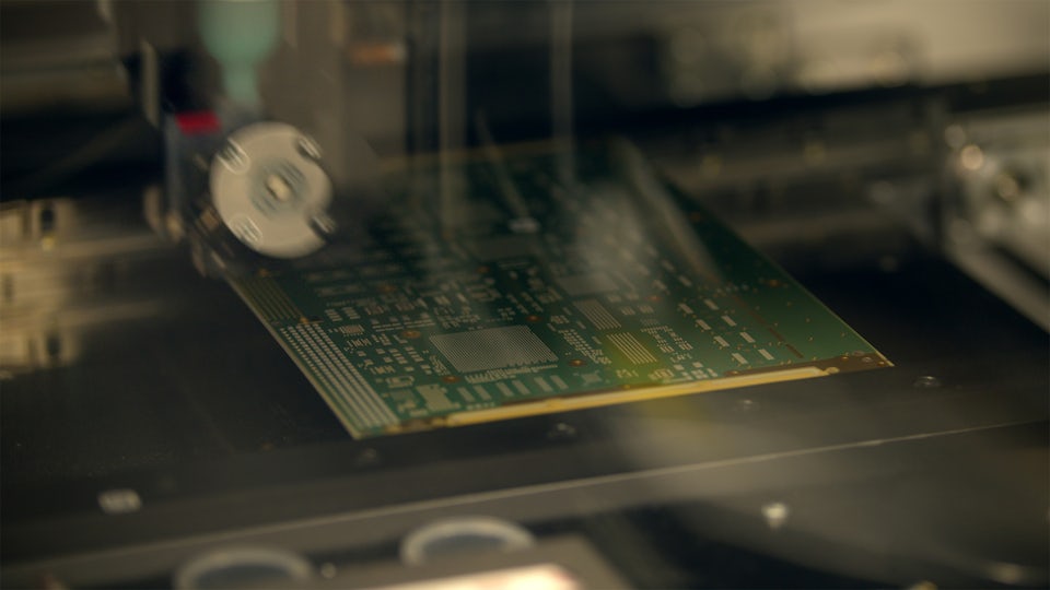
PCB design software
PCB design is an important part of the product development process, and it continues to evolve and change as electronics become more prevalent and more complex. On this page you can learn the ins and outs of PCB design software directly from the experts at Siemens.
What is PCB design software?
PCB design software refers to computer applications specifically designed to facilitate the creation, layout, routing, simulation, and analysis of printed circuit boards (PCBs). These software tools provide a platform for engineers to complete PCB designs. What is PCB design? Learn more in our blog!

Why is PCB design software important?
Device functionality
PCB design software helps ensure that these components like microprocessors, memory & sensors work together and that the device will work as intended.
Product size
PCB design plays a role in determining the size and form factor of electronic devices. Compact and efficient PCB layouts done in PCB design software allow for smaller and more portable devices.
Signal Integrity
PCBs are responsible for routing signals between components. The right PCB design software can help you design boards that minimize signal interference, ensuring data and power transmission is reliable and stable.
What can PCB design software do for you?
PCB design software should deliver the functionality you need, like layout and schematic, but also go beyond to enable a fully integrated electronic systems design flow that bridges the gap from design to manufacturing with integrated verification at every step.
Full system connectivity
Establish a digital thread that seamlessly connects the entire system, including subsystems and functional partitions across multiple engineering domains, on a unified platform. Ensure transparent and traceable data linkages.
Enhanced supply chain resilience
Enable a complete digital thread from component OEM to final product, providing valuable insights into the supply chain and supporting trust and traceability initiatives.
Secured design data linkages
Create a digital twin for electronics design, linking it with mechanical, electrical, and software data for a full digital thread, ensuring data integrity and security throughout the product lifecycle.
Accelerated time-to-manufacturing
Implement a design-to-manufacturing digital thread that optimizes production processes and ensures full product and process traceability, leading to faster time-to-market.
PCB design software from Siemens


PCB design best practices
Today, PCB design teams must deliver more complex products on even more compressed schedules. Get ahead of these challenges by learning the best practices of modern PCB design, which we have broken down by five pillars of digital transformation.

Digitally integrated & optimized
Establishing a digitally integrated solution across multiple engineering domains reduces manual intervention, fosters collaboration and improves transparency across disciplines. Learn more about how to create a digitally integrated and optimized multi-domain environment.

Engineering productivity
Using today’s PCB design tools like Xpedition can significantly optimize the design approach and facilitate multi-discipline integration and collaboration so that you can be faster, produce higher quality designs, and even lower project risks.

Digital verification
Shift-left design methodology integrates design verification tools throughout the PCB design process to let designers find and fix errors where they happen, instead of waiting until later.
.png?auto=format,compress&fit=max&w=720)
Model-based systems engineering
A digital thread breaks down barriers between teams and establishes traceability from requirements all the way through manufacturing and across multiple design domains. A digital twin allows teams to perform simulations early, enabling trade-off analysis and optimized system integration.

Supply chain resilience
Electronic systems design companies have always depended on a value chain of suppliers and manufacturing services to bring successful products to market. Connecting the demand for a product with the supply of its necessary parts has never been more complex than it is today.
Abaco Systems | AMETEK
Facilitating product innovation through tools, processes, and people
Company:Abaco Systems | AMETEK
Industry:Electronics
Location:Huntsville, Alabama, United States
Siemens Software:HyperLynx, Valor NPI, Xpedition Enterprise
The tools themselves are a very important aspect of what we do here. It may be that a lesser tool could be employed but the time scales involved in that would just be horrific. We need the fastest most efficient tools that we can have to get our very complex designs to market on time. We get that from the Siemens tools.
Frequently asked questions
Learn more
Watch
Watch the PCB design best practices video series to optimize tools and processes throughout the full PCB design process.
Read
Read the electronic systems design blog