IC packaging design and verification
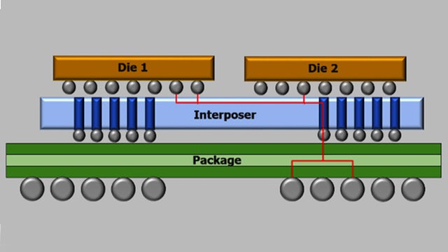
Monolithic scaling limitations drive the growth of 2.5/3D multi-chiplet, heterogeneous integration that enables PPA targets to be met. Our integrated flow addresses IC package prototyping challenges to signoff for FOWLP, 2.5/3D IC and other emerging integration technologies.
IC Packaging Design tools provide a complete design solution for creating complex, multi-die homogeneous or heterogeneous devices using FOWLP, 2.5/3D or system-in-package (SiP) modules, as well as IC package assembly prototyping, planning, co-design and substrate layout implementation.
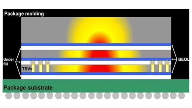
Analysis of die/package signal and power integrity, EM coupling and thermal conditions. Fast, easy-to-use and accurate, these tools ensure that engineering intent is fully achieved.
Physical verification and signoff that meet foundry and outsource substrate assembly and test (OSAT) requirements ensure performance and time-to-market goals are met.
3D IC Podcast
Take a deep dive into the 3D IC podcast series to learn how three-dimensional integrated circuits take less space and deliver higher performance.


