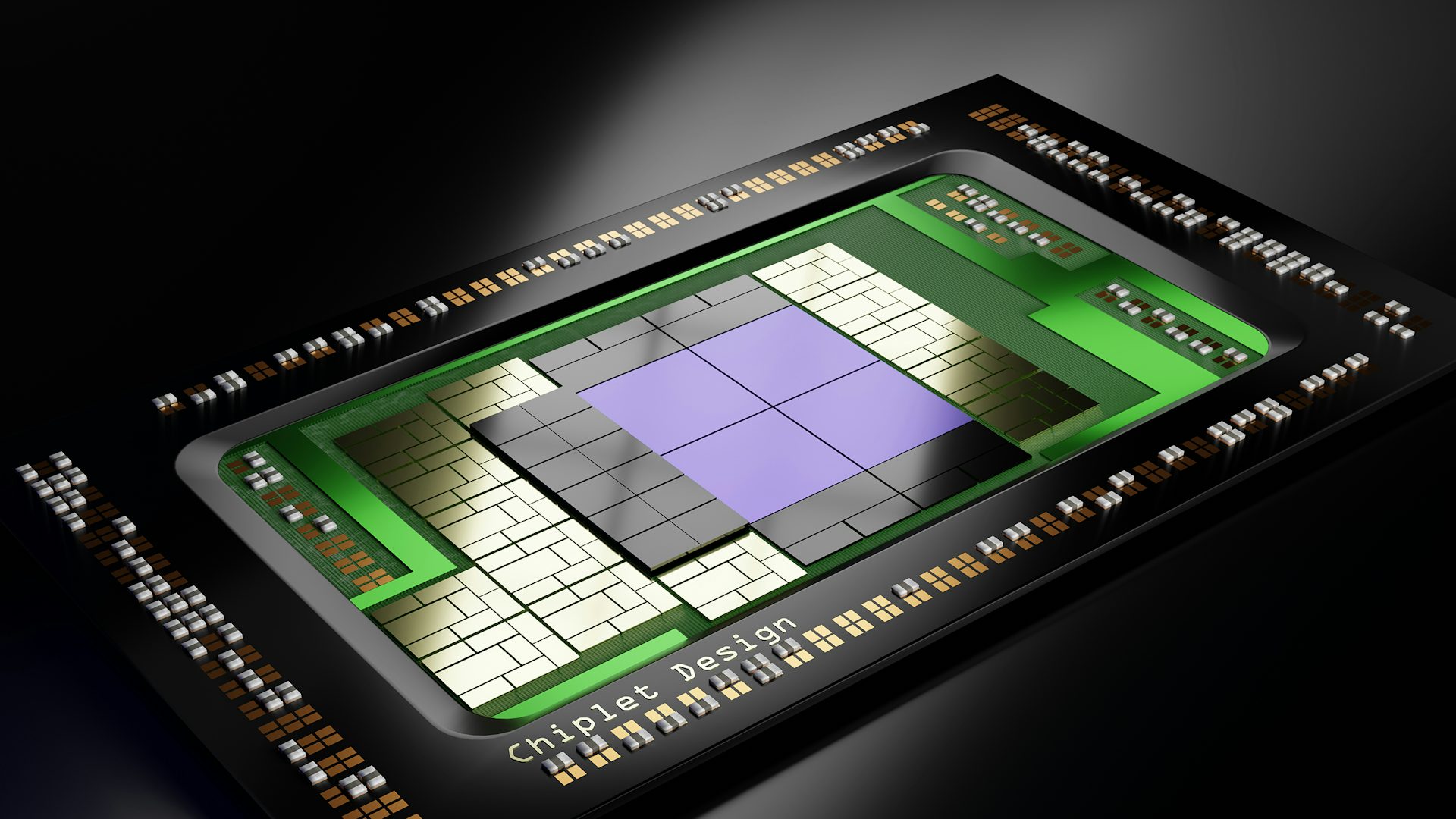
Why Tessent Multi-die?
Dramatically speed and simplify critical design-for-test (DFT) tasks for next-generation integrated circuits (ICs) based on 2.5D and 3D architectures with Tessent Multi-die.
Solve complex 3D stacking challenges
Tessent Multi-die provides a comprehensive DFT automation solution for highly complex tasks associated with 2.5D and 3D IC designs and works seamlessly with Tessent TestKompress, Streaming Scan Network and IJTAG software.
Seamless integration
Tessent Multi-die seamlessly integrates with other Tessent products using an integrated Tessent platform.
Automate 3D IC DFT
Faster, simpler DFT enables IC design teams to generate compliant hardware rapidly. DFT technology that keeps pace with multi-dimensional designs allows for quicker test implementation and optimized manufacturing test costs.
Solving Test Challenges of Multi-die Designs
Watch as Vidya Neerkundar, Tessent Product Manager, explains how Tessent Multi-die enables fully automated implementation of DFT for designs that scale sideways (2.5D devices), are stacked on top of one another (3D), or combine both configurations and how the architecture for each die can stay independent regardless of what logic needs to be tested within or across the dies.
3D IC design solutions
Explore and deliver product differentiation faster using 3D heterogeneous integration of node and performance-optimized chiplets with Siemens EDA's market-leading 3D IC technology solution.

Affordable/comprehensive DFT of 3D stacking die devices
Facing manufacturing limitations with respect to die sizes? These advanced designs already push current design-for-test solutions to the limits. In this paper, we outline a path to scalable DFT solutions into the third dimension to deliver an affordable and comprehensive answer to this question.


.png?auto=format,compress&w=640&h=360&q=60&fit=crop)


