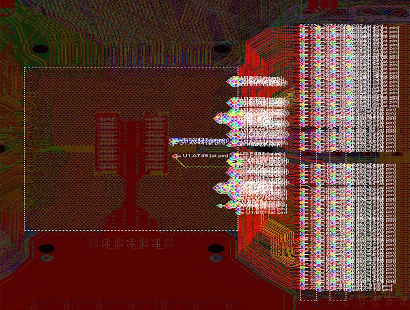
DDR interfaces contain multiple groups of signals, each with unique signal quality requirements. They also have relative timing relationships between signal groups that need to be satisfied. All of the signals in all of the groups need to be analyzed to ensure that the design will work as intended. In the image shown here, there are over 64 signals, including clock, command/address, data, data strobe and status. A signal quality or timing problem with any single signal has the potential to render the entire interface inoperable.
Fortunately, DDR interfaces are associated with JEDEC specifications that document interface requirements - but only for the DRAM side of the interface. JEDEC does not specify controller I/O signal or timing requirements, so different controllers will have unique behaviors that have to be taken into account during analysis. For example, controllers might perform deskewing on an interface, byte, nibble or individual bit basis - or not at all.
Ensuring that an interface will work requires ensuring that signal quality and timing requirements are met for all signals and inter-group relationships, including controller-specific behaviors. This requires simulating all signals and post-processing waveform data to extract eye measurements and interconnect flight times for use during timing calculations. Performing this analysis for a complete DDR interface is difficult, since there are dozens of signals involved. Ideally, this analysis should be fully automated, because of the complexity and number of analysis steps involved.


