Our ongoing collaboration with TSMC has successfully resulted in automated workflow certification for their InFO integration technology that is part of the 3DFabric platform. For mutual customers, this certification allows the development of innovative and highly differentiated end-products using best-in-class EDA software and industry-leading advanced packaging integration technologies.
Our automated InFO_oS and InFO_PoP design workflows are now certified by TSMC. These workflows include Innovator3D IC, Xpedition Package Designer, HyperLynx DRC, and Calibre nmDRC technologies.
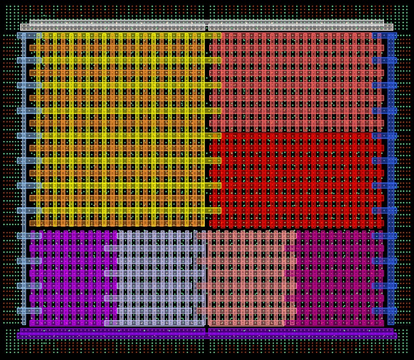
Integrated Fanout (InFO)
As defined by TSMC, InFO is an innovative wafer level system integration technology platform, featuring high density RDL (Re-Distribution Layer) and TIV (Through InFO Via) for high-density interconnect and performance for various applications, such as mobile, high performance computing, etc.. The InFO platform offers various package schemes in 2D and 3D that are optimized for specific applications.
InFO_oS leverages InFO technology and features higher density 2/2µm RDL line width/space to integrate multiple advanced logic chiplets for 5G networking application. It enables hybrid pad pitches on SoC with minimum 40µm I/O pitch, minimum 130µm C4 Cu bump pitch and > 2X reticle size InFO on >65 x 65mm substrates.
InFO_PoP, the industry's 1st 3D wafer level fan-out package, features high density RDL and TIV to integrate mobile AP w/ DRAM package stacking for mobile application. Comparing to FC_PoP, InFO_PoP has a thinner profile and better electrical and thermal performances because of no organic substrate and C4 bump.
Chip on Wafer on Substrate (CoWoS)
Integrates logic and memory in 3D targeting, AI, and HPC. Innovator3D IC creates, optimizes & manages a 3D model of the entire CoWoS device assembly.
Wafer on Wafer (WoW)
Innovator3D IC creates, optimizes, and manages a 3D digital twin model that drives detailed design and verification.
System-on-Integrated-Chips (SoIC)
Innovator3D IC optimizes and manages a 3D digital twin model that drives design and then verification with Calibre technologies.