Z-planner Enterprise stackup wizard

PCB stackup design wizard

Z-planner Enterprise comes equipped with an advanced stackup wizard that allows users to design and refine a multi-layer stackup quickly and comprehensively. Explore the capabilities of the Z-planner Enterprise stackup wizard in the free online trail.

Building a PCB stackup with Z-planner Enterprise

Building a stackup using the stackup wizard consists of altering 4 basic attributes:

  • Copper Layer Creation
  • Impedances
  • Vias
  • Dielectrics

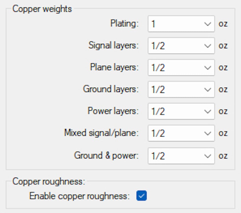
Copper layer creation

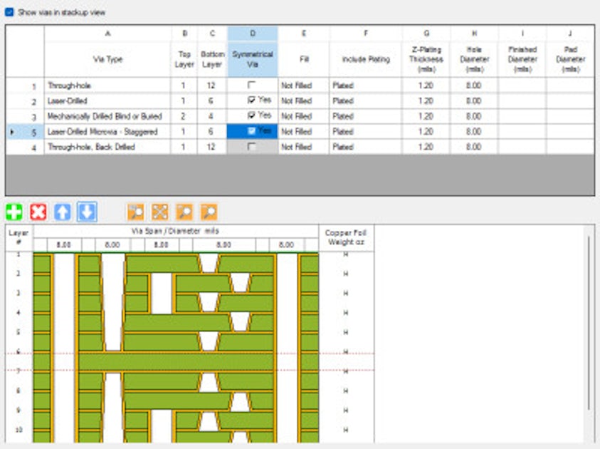
Z-planner Enterprise is useful for defining sequentially laminated HDI stackups.

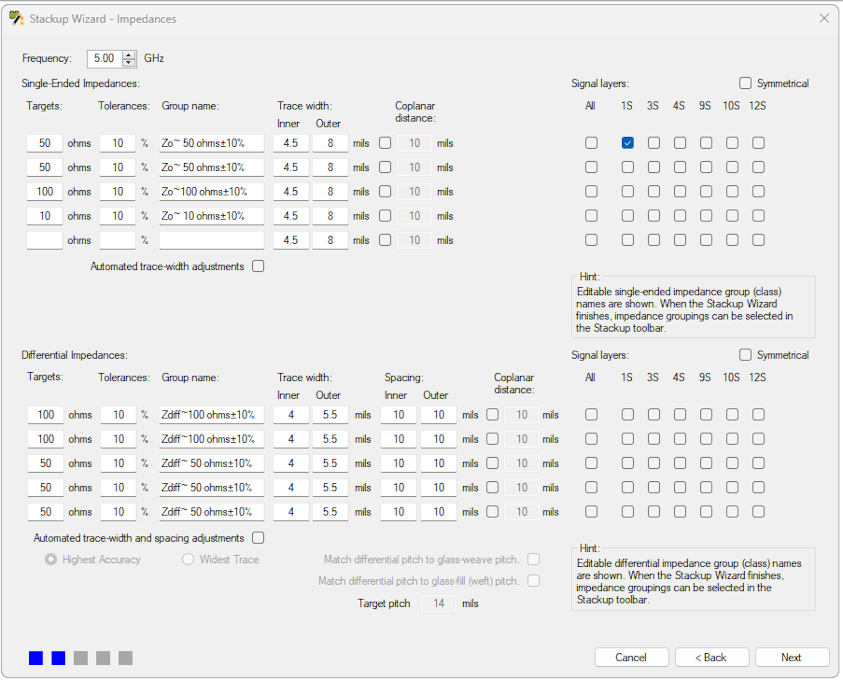
The stackup wizard generates an optimized stackup based on the number, sequence and copper weight of individual layers as they correspond to copper weight, trace width, spacing and etchback values. Z-planner Enterprise can generate stackups with a standard single lamination cycle or create a sequentially laminated stackup, including blind and buried via fabrication, multiple prepregs on build-up layers, as well as the associated plating.

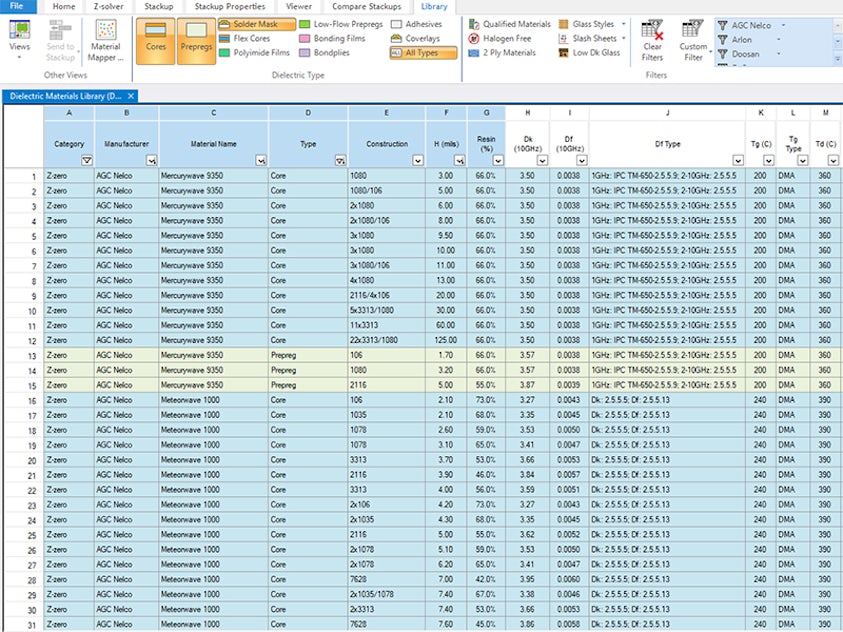
Z-planner Enterprise’s materials library contains copper (Cu) roughness values for both sides of the foil as measured in Rx (um) values.

copper weight selection within the Z-planner Enterprise stackup wizard tool

Impedance

The stackup wizard allows users to create single-ended and differential-impedance groups for each stackup in the wizard. For differential signals, a stackup can be optimized for either the highest possible accuracy, or to favor wider traces.

Z-planner Enterprise is designed with Signal Integrity (SI) in mind, helping users to mitigate the affects of Glass Weave Skew during the design of the stackup, before a single trace has been laid. Z-planner Enterprise does this by providing dielectric material recommendations and layout preferences designed to mitigate the fiber weave effect.

The stackup wizard allows users to create single-ended and differential-impedance groups for each stackup in the wizard.

Vias

Designing via placement is crucial before calculating impedances, as via plating adds to the overall copper foil thickness in the manufactured board.

By default, a through-hole via is included within the default design. In addition to this, Z-planner Enterprise allows users to define other via structures, including blind and buried vias or back drilled vias.

The plating process is what separates vias from holes, and plating will be suggested by the wizard for new vias. Top and bottom layers for each via can also be defined, and plating thickness can be edited manually. If prepregs are required to produce the required via configuration, the starting layers will be automatically adjusted.

Vias that begin on non-outer layers will have the following attributes that are different from normal copper layers:

  • Copper foils for via starting layers will be provided by the PCB fabricator and will be standard “HTE" foil by default (Rz~8.5 um). This is important for designs concerned about signal loss, as foil used on build-up layers will be much rougher than what may be selected with the chosen laminate.
  • Plating will be added to via starting layers. Fortunately, plating is smoother (Rz~3 um) than HTE copper, and all of this is tracked and managed by Z-planner Enterprise.
  • Prepregs are required, and will be added automatically, for via starting layers.
via creation for a PCB stackup within the Z-planner Enterprise stackup wizard

Dielectrics

The Z-planner Enterprise stackup wizard allows a user to generate a stackup using known materials, a material from a known manufacturer, or to optimize based on known material parameters such as Dk, Df or Tg. Depending upon the method used, the wizard makes some suggested constructions based on materials within the library. Regardless of the generated materials, specifications and calculations, all aspects of the generated stackup are editable after completing the wizard.

Z-planner Enterprise dielectric material library