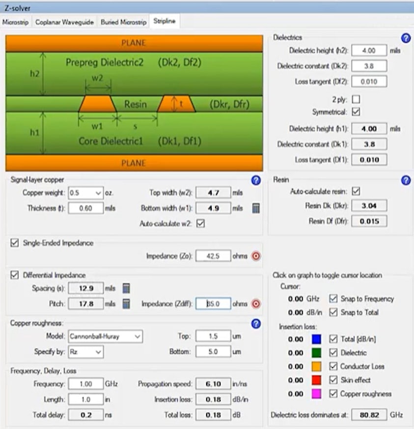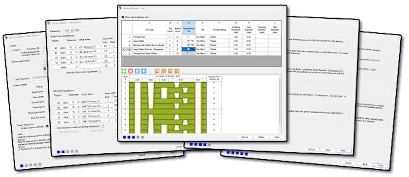
PCB stackup calculator
Z-planner Enterprise contains a stackup calculator which ensures signal integrity across a
PCB for various controlled impedance models to quickly simulate electrical performance based on the current stack up configuration.
Making use of Siemen’s Hyperlynx Field Solver, users are able to target specific differential impedances to determine specific circuit values based off of the copper trace specs and the calculated signal frequency characteristics.
Insertion loss
Stackup planning requires more than just calculating controlled impedance. Z-planner Enterprise allows detailed insertion loss calculation within a stackup across any range of frequencies. Calculate your total insertion loss and determine specific sources for this loss including:
- dielectric loss
- copper roughness
- skin effect
- glass weave skew
- conductor loss
Dielectric dissipation factors
By altering trace length, dielectric dissipation factors and copper material attributes, Z-planner Enterprise provides you with a valuable insight into the electrical integrity of your PCB stackup design.