
Define the microvia structure and associated constraints
Specific values for via capacitance and delay are important for constraint adherence (e.g. delay formulas) and simulation accuracy.
Localized rules under components to facilitate escape paths
When doing the fanout, localized rules (trace widths/clearances, via sizes) can be defined to achieve the densities necessary to route away from the high-density pins. Using larger rules everywhere else will result in higher yield.
45° routing for BGA fanout
Routing with true 45-degree angles creates escape paths out of high-density pad regions.
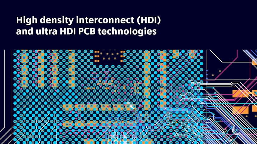
Vias inside SMD land pads
Vias inside pads help facilitate tighter densities.
Via fanout routing schemes
Unique via fanout routing schemes (define what depth to stagger to; router will create appropriate stagger pattern)
Dive deeper into this topic
If you'd like to learn more about HDI read our blog post on high density interconnect (HDI) and ultra HDI PCB technologies.