Xpedition
PADS Pro Essentials
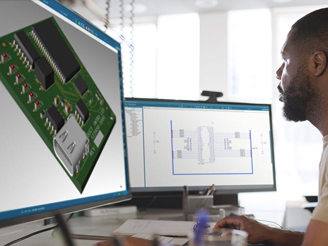
PADS Pro Essentials delivers affordable PCB design for independent engineers. The software provides professional-grade tools, easy digital access, and community-based support.
Xpedition offers scalable solutions for both simple and complex systems, featuring a shared technology base and database format across all tiers. The platform includes modern features like AI-powered productivity tools, hierarchical design capabilities, and cloud-based parts management, while ensuring seamless upgradability without requiring data translation or additional training.
PADS Pro Essentials, Xpedition Standard and Xpedition Enterprise deliver professional-grade PCB design solutions tailored for engineers, small teams and global enterprises. Whether designing simple boards or complex multi-domain systems, Xpedition has the tools, automation and collaboration capabilities needed to drive innovation, accelerate time-to-market and streamline the entire product lifecycle.

PADS Standard, PADS Standard Plus, PADS Professional and PADS Professional Premium are still current products in our portfolio. If you are interested in additional seats of PADS Standard, PADS Standard Plus, PADS Professional or PADS Professional Premium, please fill out the contact form for more information.

