Flow integration
I/O optimization is tightly integrated with the Xpedition Enterprise design flow, accessible at any stage of the project using a tab in the Xpedition schematic design environment. Schematic, PCB layout and FPGA databases are kept in sync through synchronization assistant. This allows users to better control the project’s design data flow. In addition, schematic users can decide when the FPGA data (new or updated ) is to be transferred to the PCB design. Before placement or routing is started on the PCB, the I/O optimizer allows floor planning using Xpedition project data in the floorplan window for better initial assignment. Then results can be exported to Xpedition’s layout environment. FPGA parts are managed at either the project or the enterprise library level.
Signal grouping
Signal groups can easily be created to manage the signal complexity of high pin count FPGAs and accelerate the pin assignment process. Each group may define the interfaces of particular hardware functions to be implemented later on in the FPGA. These groups may be treated as separate HDL entities within the tool. Signal groups can either be created manually through the GUI or extracted from an HDL file (Verilog or VHDL).
Pin partitioning
By grouping pins across the FPGA’s I/O banks, the optimizer provides more flexibility in pin assignment. The advantages of pin partitioning include better PCB connection planning, customized symbol generation and minimizing the pin swap rules within the group, leading to better control of pin optimization and improved net unravelling. Furthermore, Signal Groups can be assigned to a partition as a single entity, removing the need to divide signal groups between I/O banks. The GUI makes managing pin partitions within the tool intuitive and simple.
Signal and pin assignments
Manually assigning hundreds of HDL signals to FPGA pins, while still strictly adhering to the FPGA vendors’ rules is a challenge to all. To counter this, the I/O optimizer provides users with an intuitive and GUI packed with useful functions. These range from auto assignment, supervision of signal standards, assignment by simple drag and drop, support for operations on sets of objects and dynamic filtering. These make signal-pin assignment a simple operation. Every change made to the pin assignment is managed across the FPGA on board flow and is kept consistent since the optimizer is between the FPGA and PCB flows, communicating all changes made on either side.
Automated part and symbol generation
The very nature of FPGA devices requires a different approach to the symbol generation process. FPGA logic may change several times during the project and symbols must be kept consistent with those changes. Users have a set of powerful features that makes symbol creation easy, fast and error free, while still allowing full control of the symbol creation process. Compared to manual symbol creation, time is reduced from hours or days to minutes.
Floor planning
An important phase of the PCB design flow is the component placement and orientation on the board layout itself. Floor planning can be done before and during the PCB layout process. Designers have the clear advantage of being able to make FPGA pin assignment changes right from the project’s early stages.
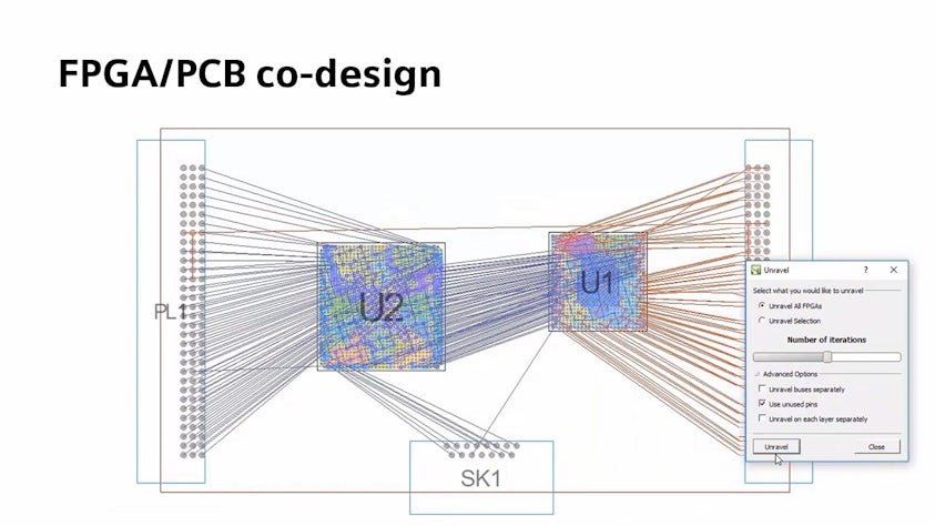
Net line unravelling
- Signal-pin assignments can be automatically optimized while respecting pin specific rules and constraints. This enables highly efficient net line unravelling, resulting in:
- Reduced number of layers
- Minimization of signal integrity issues
- Increased timing budgets
- Minimization of trace length on the PCB
- Much faster route time of the FPGA in situ on the board.
The I/O optimizer guarantees error-free pin swapping during the signal assignment process. Unravelling may be done on the Xpedition layout data or much earlier during floor planning. In addition, it is fully supported between pins, pin escapes, end-of-traces and route targets.
FPGA multi-instance
In most cases, the same FPGA device will have different logical functions shared across projects or even shared within a single project. The I/O optimizer fully supports these situations and this is done automatically during project development. FPGAs represented by different functional symbols in the BOM report are listed along with the vendor’s codes.
Multi-FPGA optimization
Successful optimization of connections between two or more FPGA devices is almost impossible to perform without this state-of-the art technology. The optimization algorithm evaluates all possible connection combinations to arrive at the optimum interconnect, minimizing net crossovers arising from the initial assignment, enabling higher route completion rates. The FPGA I/O optimizer includes multi-FPGA optimization as standard.
Dive deeper into this topic

Use a tool that enables correct-by-construction FPGA I/O assignment, allowing pin swapping and layout-based I/O optimization within the PCB design process. Read more in our FPGA-PCB co-design blog.