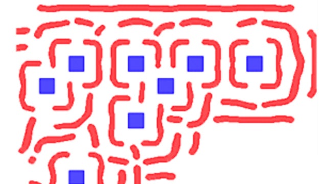
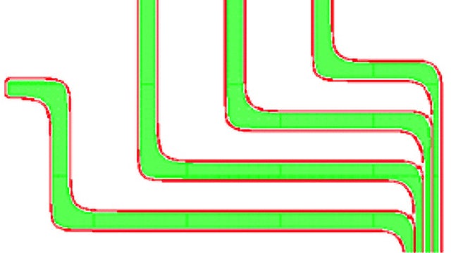
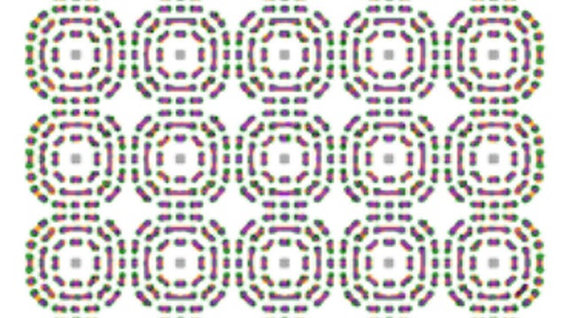
In the last decade, photonics technology has been an emerging technology for optical telecommunications and optical interconnects in microelectronics. As a result, a large diversity of photonics design methodologies has merged with very challenging scales and shapes. Manufacturing such curvy and critical photonics shapes requires advanced resolution enhancement techniques (RET), including inverse lithography techniques (ILT) with 193 nm immersion lithography. In this paper, we investigate the manufacturing challenges of several photonics devices using advanced ILT solutions and the impact of SRAF insertion on delivering good litho quality, including edge placement error (EPE), PVband, and line edge roughness (LER). We will demonstrate how our Calibre ILT solutions enable the manufacturing of the most challenging photonics designs.


