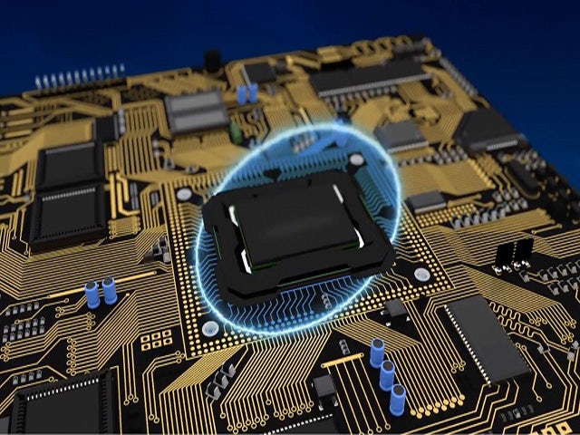
Meeting fabrication requirements
Advanced substrate technologies require complex metal-filled areas. You will have guidelines on outgassing void insertion, metal balancing and ball/bump thermal ties. Interoperability between signal routing, route tuning and all-metal area fill creation/editing operations becomes mandatory.
TECHNOLOGY OVERVIEW
Dynamically execute with tapeout results
Achieve semiconductor packaging quality thanks to interoperability between routing, tuning, and area fill operations. Automatic and interactive graduated degassing and metal balancing allow you to balance layer pairs to specified thresholds. With a multi-threaded dynamic plane engine, results are always tapeout ready with no need for postprocessing before you can create your OASIS or GDSII mask sets.

