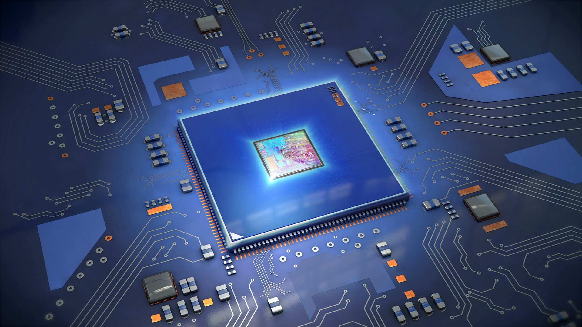
Leveraging 3D design for IC packaging efficiency
Multi chiplet/ASIC packages often use substrates for high-speed integration and ball grid arrays (BGA) for connection, including mechanical stiffeners andheat spreaders. The IC package can look like a Manhattan skyline. The ability to visualize/edit in 3D reduces errors and shrinks design cycles.
TECHNOLOGY OVERVIEW
2D and 3D delivers productivity and efficiency
Designers can view and edit their IC package designs simultaneously in 2D and 3D
