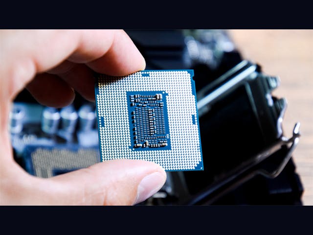
IC Packaging Design Flows
Today's high-performance products require advanced IC packaging that utilizes heterogeneous silicon (chiplets) to be integrated into multi-chip, wafer-based HDAP packages. Different vertical markets often have specific needs and corresponding design flows as shown below.
Common industry semiconductor packaging design flows
Advanced semiconductor packaging is critical to industries where high-performance is mandatory.
Systems Companies
By integrating functionality into systems-in-packages, automotive suppliers can deliver greater electronics capability in a smaller, more reliable and lower cost form factor. Companies that incorporate custom high performance semiconductor into their system PCBs, such as telecom, networking switches, data center hardware, and high-performance computer peripherals, require heterogeneous integration to meet performance, size, and manufacturing costs. A key component of the Siemens semiconductor packaging solution is Innovator3D IC where chiplets/ASICs, package, and system PCB substrate technologies can be prototyped, integrated, and optimized using the system PCB as a reference to drive package ball-out and signal assignments to provide best-in-class results.
Lower costs are also achieved by integrating functionality into systems-in-package (SiP), a fact that automotive sub-system suppliers leverage when developing mmWave technologies and products.
Defense & Aerospace Companies
Multi-chip modules (MCM) and System-In-Packages (SiP) developed in the context of their PCBs to meet performance and size requirements. Commonly utilized by military and aerospace companies in order to meet performance and size/weight requirements. Particularly important is the ability to prototype and explore the logical and physical architecture before moving to physical design. Innovator3D IC provides rapid multi-substrate prototyping and assembly visualization for MCM and SiP planning and optimization.
OSATs & Foundries
Package design and verification requires cooperation with end-product customers. By using common tools that have the integration and functionality needed to operate in both the semiconductor and packaging domains and by developing and deploying verified process-optimized design kits (such as PADK’s and PDKs), OSATs, foundries, and their customers can achieve design, fabrication, and assembly predictability and performance.
Fabless Semiconductor Companies
Semiconductor package prototyping and planning using an STCO methodologies has become mandatory as is the need for PADK/PDK from the foundry or OSATs. Heterogeneous integration is critical to markets where performance, low power, and/or size or weight are key. Innovator3D IC helps companies' prototype, integrate, optimize, and verify the IC, package, and reference PCB substrate technologies. The ability to consume PADK/PDK for manufacturing signoff is also key, and the use of Calibre technologies provides both consistency of quality and reduced risk.
3DbloxTM
TSMC’s 3Dblox language is an open standard designed to foster open interoperability between EDA design tools when designing 3DIC heterogeneous integrated semiconductor devices. Siemens is proud to be a subcommittee member and is committed to collaborate with other committee members and to drive the development and adoption of the 3Dblox hardware description language.
Learn more about designing silicon interposers
In this video, you will learn about designing silicon interposers for 2.5/3DIC heterogenous integration.