
Foundry solutions
Fabless/foundry ecosystem solutions
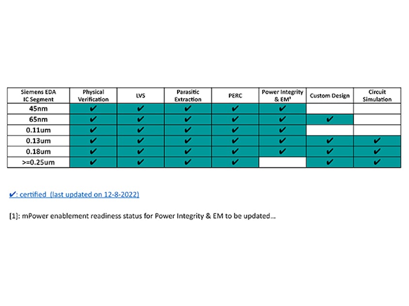
Siemens EDA tools, resources, and expertise enable the successful creation and manufacture of the most advanced and complex IC, IP, and SoC products. Proven in day-to-day operations at design companies and foundries, Siemens EDA supports fabless/foundry ecosystems with collaboration and innovation.
Foundry news


Foundry events
TSMC NA Technology Symposium 2025
Join Siemens EDA at TSMC's North America Technology Symposium in person, in Santa Clara, California Wednesday, April 23th, 2025.
April 23th, 2025
Santa Clara, CA


Foundry ecosystem collaboration
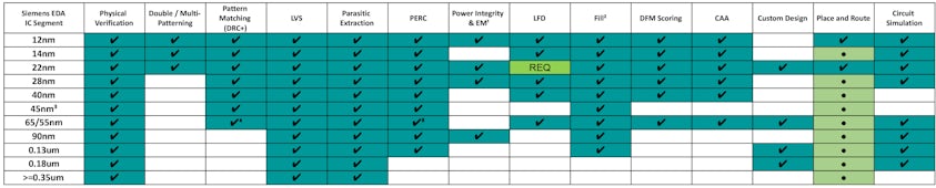
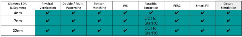
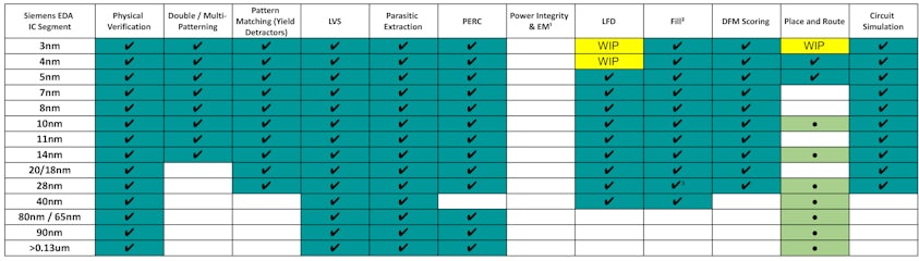
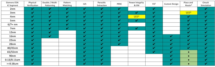
Siemens EDA tools are proven at semiconductor foundries around the globe. Collaboration with major foundries ensures the earliest access to the tools needed for advanced manufacturing processes, as well as the functionality and performance required for continued success at established process nodes.
Looking for Calibre products?
Calibre Design Solutions delivers a complete IC verification and DFM optimization platform to speed designs from creation to tapeout. Calibre Manufacturing solutions enable foundry success throughout the entire technology node lifecycle.
Ready to learn more about Calibre?
We're standing by to answer your questions! Get in touch with our team today
Call: 1-800-547-3000
Calibre consulting services
We help you adopt, deploy, customize and optimize your complex design environments. Direct access to engineering and product development lets us tap into deep domain and subject matter expertise.
Support center
The Siemens Support Center provides you with everything in one easy-to-use location -
knowledgebase, product updates, documentation, support cases, license/order information and more.
Design with Calibre blog
The Calibre tool suite delivers accurate, efficient, comprehensive IC verification and optimization across all process nodes and design styles while minimizing resource usage and tapeout schedules.