
Foundry solutions
Fabless/foundry ecosystem solutions
Siemens EDA tools, resources, and expertise enable the successful creation and manufacture of the most advanced and complex IC, IP, and SoC products. Proven in day-to-day operations at design companies and foundries, Siemens EDA supports fabless/foundry ecosystems with collaboration and innovation.
Foundry news


Foundry events


Foundry ecosystem collaboration
Siemens EDA tools are proven at semiconductor foundries around the globe. Collaboration with major foundries ensures the earliest access to the tools needed for advanced manufacturing processes, as well as the functionality and performance required for continued success at established process nodes.
GlobalFoundries
GlobalFoundries Inc. (GF) is one of the world’s leading semiconductor manufacturers, offering a unique mix of design, development, and fabrication services for both leading-edge and mainstream technologies. GlobalFoundries is redefining innovation and semiconductor manufacturing by developing and delivering feature-rich process technology solutions that provide leadership performance in pervasive high growth markets. GlobalFoundries and Siemens EDA frequently collaborate on a wide range of projects to enhance the productivity and outcomes of design, verification, and manufacturing processes for their mutual customers.
GlobalFoundries coverage table
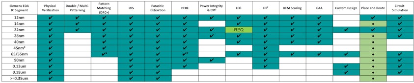
✔: certified; REQ: by service request only (last updated on 12-7-2022)
[1]: Only mPower Digital is enabled and certified for GF process nodes.
[2]: Calibre SmartFill is POR (Plan of Record) below 20nm and Dummy Fill above 20nm.
[3]: 45nm process node supports RF SOI CMOS technology specifically.
[4]: 55nm has a DRC+ kit but 65nm does not.
[5]: Calibre PERC deck is available for 55LP PDK only but not for other 65/55nm PDKs.
●: Tech files would be provided by Siemens for those process nodes not certified. Please contact Aprisa product team for your requests.
Intel Foundry Services
Intel Foundry Services (IFS) offers a wide range of manufacturing services to meet your unique product needs, from mask generation to wafer manufacturing to industry-leading sort and test capabilities. Intel’s advanced packaging techniques allow integration of diverse computing engines across multiple process technologies with performance parameters similar to a single die, but with a platform scope that far exceeds the die-size limit of single-die integration. As a global leader in research and development (R&D) and manufacturing, Intel continuously seeks to optimize and deliver industry-leading platform solutions with our customers for every existing and evolving market segment.
The IFS Accelerator - EDA Alliance is committed to establishing an ecosystem for the design and fabrication of next generation system-on-chip (SoCs) manufactured on IFS leading-edge process technologies. The initiative promotes collaboration between IFS and its ecosystem partners, with a focus on reducing risk and tackling design barriers while accelerating time-to-market for mutual customers’ products. As part of the alliance, Siemens EDA will collaborate closely with IFS to optimize its best-in-class IC design tools, flows, and methodologies for Intel’s world-class processes.
IFS Accelerator - EDA Alliance
Intel Foundry Services coverage table
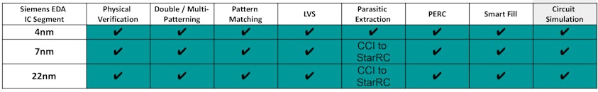
✔: certified (last updated on 12-6-2022)
Samsung Foundry
Samsung Foundry offers competitive processes, design technologies, IP, and high-volume manufacturing capability for customers with a full suite of advanced process technologies, including integrated package solutions for 3D/2.5D and flexible and efficient cloud-based design environments. As a partner in the Samsung Advanced Foundry Ecosystem (SAFE™) program, Siemens EDA engages in joint projects with Samsung Foundry to enable the advanced platforms and technologies their mutual customers rely on to bring increasingly sophisticated designs to life.
Samsung coverage table
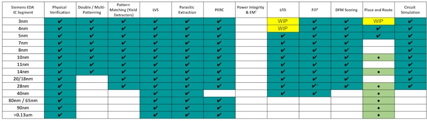
✔: certified; WIP: work in progress (last updated on 4-29-2023)
[1]: mPower enablement readiness status for Power Integrity & EM to be updated…
[2]: Calibre SmartFill is POR (Plan of Record) below 20nm and Dummy Fill above 20nm.
[3]: Calibre SmartFill deck is available for 28FDS PDK only but not for other 28nm PDKs.
●: Tech files would be provided by Siemens for those process nodes not yet certified. Please contact Aprisa product team for your requests.
TSMC
The Taiwan Semiconductor Manufacturing Company (TSMC) pioneered the pure-play foundry business model. By choosing not to design, manufacture or market any semiconductor products under its own name, the key to TSMC’s success has always been to focus on its customers’ success. TSMC-made semiconductors serve a global customer base that is large and diverse, with a wide range of applications used in a variety of end markets, including smartphones, high performance computing, the Internet of Things (IoT), automotive, and digital consumer electronics.
The TSMC EDA Alliance reduces design barriers for customer adoption of TSMC process technologies. As an EDA Alliance partner, Siemens EDA works closely with TSMC's design technology teams to address mutual customer design needs through the enablement of new EDA tool features that align with TSMC advanced process development roadmap, as well as the implementation of TSMC's design methodology in reference flows. Through this collaboration, TSMC and Siemens EDA enable mutual customers to better achieve their PPA target in a shorter period of time.
TSMC coverage table
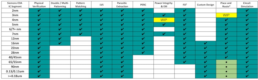
✔: certified; WIP: work in progress (last updated on 4-29-2023)
[1]: Calibre SmartFill is POR (Plan of Record) below 20nm and Dummy Fill above 20nm.
●: Tech files would be provided by Siemens for those process nodes not yet certified. Please contact Aprisa product team for your requests.
Tower Semiconductor
Tower Semiconductor offers advanced analog technologies and manufacturing solutions for the forefront of the world’s most exciting and growing arenas, such as automotive, consumer, medical, industrial, and aerospace and defense, among others. Tower Semiconductor specializes in customized analog solutions for manufacturing differentiated products, offering cutting-edge process technologies including radio frequency (RF), high performance analog (HPA), integrated power management, CMOS image sensors (CIS), non-imaging sensors (NIS) and mixed-signal CMOS, as well as micro-electro-mechanical systems (MEMS) capabilities. To complement its advanced technology platforms, the Company also offers design enablement services, providing mature and valuable tools that enable a quick and accurate design cycle.
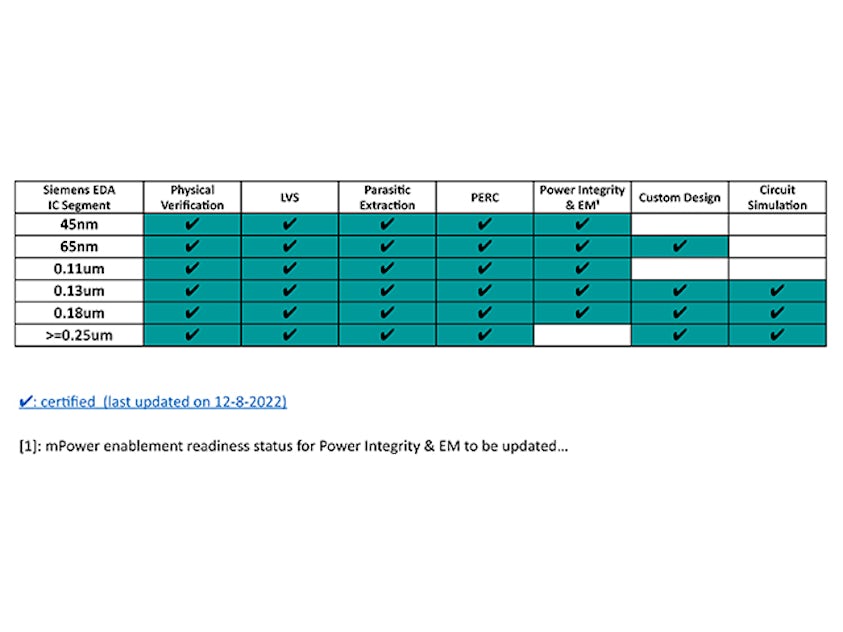
✔: certified (last updated on 12-8-2022)
[1]: mPower enablement readiness status for Power Integrity & EM to be updated…
Ready to learn more about Calibre?
We're standing by to answer your questions! Get in touch with our team today:
Call: 1-800-547-3000
Calibre Consulting Services
We help you adopt, deploy, customize and optimize your complex design environments. Direct access to engineering and product development lets us tap into deep domain and subject matter expertise.
Support Center
The Siemens Support Center provides you with everything in one easy-to-use location -
knowledgebase, product updates, documentation, support cases, license/order information and more.
Design with Calibre blog
Across all process nodes and design styles, the Calibre toolsuite delivers accurate, efficient, comprehensive IC verification and optimization, while minimizing resource usage and tapeout schedules.